EE 201P
Digital Electronics Laboratory II
|
I. Objectives
(a) Design and implement an asynchronous mod 5 counter using clear terminals.
(b) Design and implement a synchronous counter for a given set of sequence.
II. Components Required
The required circuit(s) should be implemented as per problem statements using TTL ICs. You can use Quad/Dual JK Flip Flop (7473)/(74273) and NAND gates (also D flip flops).
III. Experimental Procedure
Part A
1. Connect a mod 5 asynchronous counter as shown in the following figure. The NAND gate output should be connected to the asynchronous clear inputs of each of the flip flops. Connect an LEDs to the outputs (A, B and C) of the flip-flops. The J and K inputs of all flip-flops must be connected to high ( + Vcc) supply.
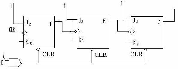
2. Connect the TTL supply from the function generator to the CLK input shown in above figure.
3. Connect the A, B, C, outputs to the LEDs and verify the execution of this circuit as mod 5 asynchronous counter. Draw the state transition diagram of the observed counter.
4. Display the waveforms of the input CLK, output at A, B, and C and also at the output of the NAND gate. Observe whether there is any spike or glitch (before clearing all the flip-flops).
Part B
1. Design a synchronous counter that has the following sequence: 000, 011, 111, 101,110 and repeats itself. The undesired (unused) states 001, 010, and 100 must always go to 000 on the NEXT clock pulse (so as to eliminate the lock out problem).
2. Compute the minimum number of flip-flops required to design above counter.
3. Implement the synchronous counter using JK flip flops (for students/groups with even bench/table numbers) or D flip flops (for students/groups with odd bench/table numbers) and some additional logic gates.
4. Display the waveforms on CRO and verify that it is working as a mod 5 synchronous counter.
The required counter circuit must be designed before arriving in the lab. Only those students who have bought the designed circuit will be allowed for experiments.
IV. Other Pre-Lab Exercises
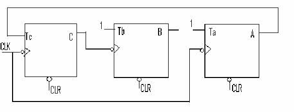
1. Analyze the following circuit and obtain the sequence of states for the first eight CLK inputs. Assume initial state as 000 (C as MSB and A as LSB).
2. Redesign mod 5 asynchronous counter using preset terminals, and observe the difference between the occurrence of states with PART A.
3. You have to convert 50MHz clock signal into 100MHz clock signal. Which type of circuit design, i.e. combinational or sequential, you will select (you must use minimum hardware)? Show the circuit diagram and clearly mention all the assumptions you have made.
Please make sure that you have shown the result of your implementation to the lab instructor (or TA) and obtained his/her signature. The two partner's in each group must obtain the signatures and attach with the lab/experiment report.