EE 201P
Digital Electronics Laboratory II
|
I. Objectives
- Analysis of 4-bit serial-in-serial / parallel out shift register.
- Implementation of a general 3-bit shifter.
II. Components Required for part ‘b’
1. D flip-flop (3) – 74HC74
2. 8 × 1 multiplexer (3) – 74HC151
III. Experimental Procedure
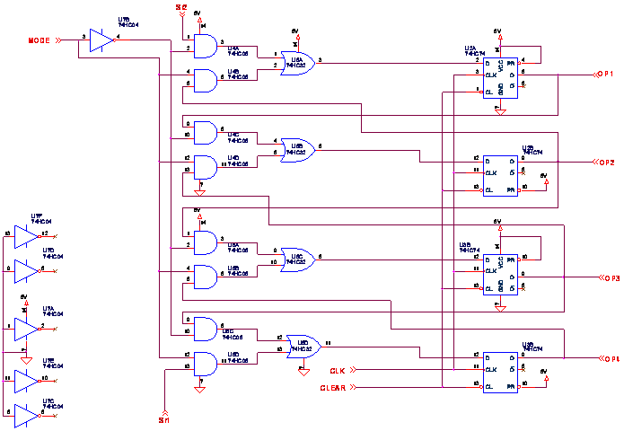
- Analyze the circuit shown in the following figure;

1. Complete/Fill in the following operation table with reference to the above shown circuit.
|
INPUT |
OUTPUT |
Mathematical operation that can be
performed, along with any
limitations on input data. (If any) |
|||||
|
CLEAR |
CLK (Edge) |
MODE |
OP4 |
OP3 |
OP2 |
OP1 |
|
|
|
|
|
|
|
|
|
|
|
|
|
|
|
|
|
|
|
|
|
|
|
|
|
|
|
|
b. Implementation of a general 3-bit shifter
1. Design general 3-bit shifter that performs the following operations:
No change in output data.
Synchronous clear
Synchronous set
Shift right
Shift left
Parallel load
Ring counter
Johnson counter
HINT: It is quite similar to the above circuit (in part a) but the input of D-FFs is the output of multiplexer.
3. Explain how the circuit can be used to implement the following shift registers:
i. SISO
ii. SIPO
iii. PISO
iv. PIPO
IV. Other Pre-Lab Exercises
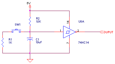
1. Study the following circuit and explain its working. What problem it solves? Study the functioning of Schmitt gates.

Please make sure that you have shown the result of your implementation to the lab instructor (or TA) and obtained his/her signature. The two partner's in each group must obtain the signatures and attach with the lab/experiment report.