EE 201P
Digital Electronics Laboratory II
|
I. Objectives
Implementation of 4-bit arithmetic circuit using 4 to 1 multiplexers and a 4 bit adder.
II. Components Required
III. Experimental Procedure
1. The functional requirement of the arithmetic adder is summarized in the table below:
|
OPERATION
SELECT |
INPUT |
OUTPUT |
OPERATION |
||
|
S1 |
S0 |
Cin |
Y |
D = A + Y + Cin |
|
|
0 |
0 |
0 |
B |
D = A + B |
Add |
|
0 |
0 |
1 |
B |
D = A + B + 1 |
Add with carry |
|
0 |
1 |
0 |
\B |
D = A + \B |
Subtract with borrow |
|
0 |
1 |
1 |
\B |
D = A + \B + 1 |
Subtract |
|
1 |
0 |
0 |
0 |
D = A |
Transfer A |
|
1 |
0 |
1 |
0 |
D = A + 1 |
Increment A |
|
1 |
1 |
0 |
1 |
D = A - 1 |
Decrement A |
|
1 |
1 |
1 |
1 |
D = A |
Transfer A |
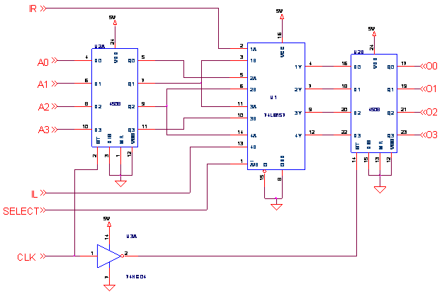
2. Realize the following circuit diagram on the PCB use LED indicators to monitor the output.

3. Verify that the circuit performs according to the description in the operation table.
4. Carefully examine and verify the functioning of the yellow colored rows (Last 2 rows) in the operation table.
IV. Other Pre-Lab Exercises
1. Study the datasheets of the ICs used in the circuit shown in following figure.
2. Explain the functioning of the circuit with the operation table and wave diagram.
Please make sure that you have shown the result of your implementation to the lab instructor (or TA) and obtained his/her signature. The two partner's in each group must obtain the signatures and attach with the lab/experiment report.