EE 201P
Digital Electronics Laboratory II
|
I. Objectives
- Analysis of serial bit stream adder.
- Design of serial adder using state machine approach.
II. Components Required (for part b)
- D flip-flop – 74HC74
- XOR gate – 74HC86
- AND gate – 74HC08
- OR gate – 74HC32
NOTE: One may use other components depending upon the design approach followed.
III. Experimental Procedure
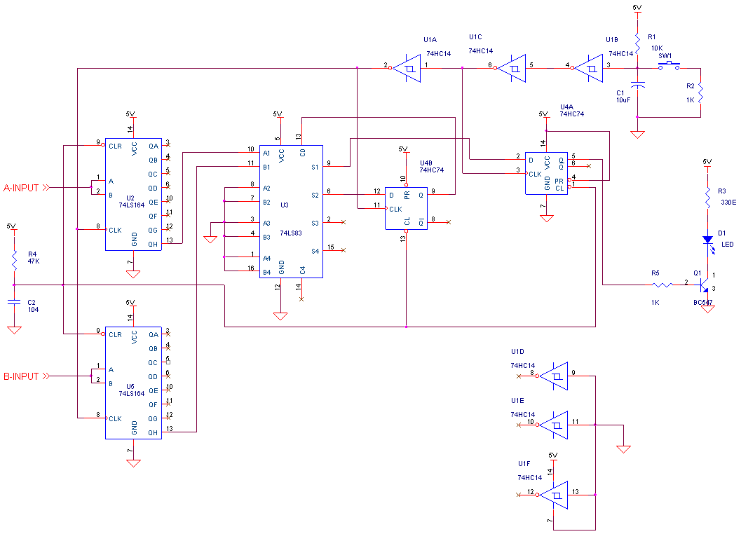
- Analyze the following circuit:

Answer the
following questions with reference to the above circuit diagram:
1. What will be the status of the 2 flip flops at power on?
2. What will be the value of U2 and U6 at power on?
3. Take any arbitrary values for inputs “A-INPUT” and “B-INPUT” (10 Bit word each). What will be the value of U2 and U6 after 8th press of the switch “SW1”?
4. Write down the status of the LED upto 19th switch press.
(The transistor “Q1” is just a LED driver i.e. LED glows if the output of “U4A” is HI and LED is off if the output of “U4A” is LOW)
b. Design of serial adder using state machine
approach.
1. Design guidelines:
· Draw the state machine for the serial bit stream adder, with each state defining the current Carry and Sum values of the addition.
· By looking at the state machine fill up the following truth table.
|
INPUT |
OUTPUT |
|||
|
A |
B |
Carry (t) |
Carry (t+1) |
SUM |
|
|
|
|
|
|
|
|
|
|
|
|
|
|
|
|
|
|
|
|
|
|
|
|
|
|
|
|
|
|
|
|
|
|
|
|
|
|
|
|
|
|
|
|
|
|
|
|
· Make K – maps for the outputs.
· Solve the K – maps to get the minimized functions.
· Use D flip flops in the circuit implementation.
· Draw the circuit diagram.
· Implement the design in the lab to verify the correctness.
IMP: The design of the circuit in part b has to be made before coming to lab and is part of the pre–lab exercise
IV. Pre-Lab Exercises
- Design of the circuit as detailed in part b of section III above.
Please make sure that you have shown the result of your implementation to the lab instructor (or TA) and obtained his/her signature. The two partner's in each group must obtain the signatures and attach with the lab/experiment report.